Andrew Bryars, Product Manager – XP Power
Currently, it is increasingly common to receive medical care and monitoring outside the usual places, such as hospitals, clinics or doctor's offices. This alleviates pressure on clinical settings due to the increasing availability of medical procedures and the aging of the world's population, which has increased the number of older people in need of medical care.
Home healthcare offers a more relaxed treatment experience by reducing stress and anxiety for patients. The new technology also makes it possible to have cosmetic applications at home.
During the Covid-19 pandemic, there was a notable boom in home health care due to a lack of beds and the desire to keep Covid patients as separated from the rest of the population as possible.
This development reached a market that was already expanding with the advent of more compact equipment and greater connectivity that offered the possibility of remote monitoring for medical teams. In the US alone, up to $265 million in services currently provided in medical centers could be referred to homes by 2025, according to McKinsey & Company.
In this context, home monitoring, diagnostic and therapeutic equipment represents more than half of the demand, making it a relevant and growing market.
Power supply for home health care equipment
As new features are added to home healthcare devices, more power is required from the power supply. Some of the newer products are already in the higher range of power delivered by external sources.
External mounting of the power supply has several advantages. The main one is that protective isolation, essential for devices connected to patients, is no longer a concern for the manufacturer since they deliver equipment previously certified by a power supply specialist.
To maintain portability and convenience, designers are challenged to provide higher wattages in units that are only slightly larger than their lower wattage predecessors. The most noteworthy aspects in this challenge are power density and thermal management, since heat removal requires resorting to devices such as heatsinks that increase size, weight, and cost.
As power designers will know, the way to reduce wasted heat is to optimize power supply efficiency. However, this level of efficiency may not be feasible with silicon (Si)-based semiconductors.
Wide bandgap technology
The need to provide higher levels of power in small solutions is not unique to home healthcare. Designers of solutions for electric vehicles and renewable energy, among others, face similar challenges and are increasingly turning to so-called wide bandgap (WBG) technology to overcome the limitations of silicon.
This “band gap” refers to the difference in energy between the top of the valence band and the bottom of the conduction band. In devices made of silicon carbide (SiC) or gallium nitride (GaN), this bandgap is significantly higher, allowing power devices to operate at higher voltages, temperatures, and frequencies.
In GaN devices, the breakdown voltage is about 30 times higher than for Si. This makes it possible to increase the doping levels and therefore decrease the conduction resistance between drain and source (RDS(ON)), which in turn reduces conduction losses and the corresponding generation of wasted heat.

Figure 1: GaN offers the lowest conduction resistance for a given breakdown voltage of all currently used materials.
Semiconductor devices also suffer losses during the switching process since the current begins to flow while the drain-source voltage (VDS) is still high. However, since GaN devices can switch faster, these losses are significantly reduced when compared to Si or even SiC.
To avoid cross tripping (shoot through), which is the creation of a short circuit during switching when a dead time occurs in which both switches are off, it is a half bridge configuration and current continues to flow during this time. In Si devices, it does so through the structural diode, whose losses are relatively high compared to GaN, whose devices do not have a structural diode, so the current flows through RDS(ON). This allows operation to be more efficient.
As a result of the lower switching losses, GaN-based power supplies can operate at higher frequencies, typically 200 kHz minimum, which is more than double that of a Si-based solution operating in the 60- 100kHz. This increase in switching frequency allows the size of the transformer, inductors and output capacitors to be significantly reduced.
Because less wasted heat is generated and GaN devices can run at a higher temperature while maintaining reliability, the need for thermal management devices such as heat sinks, frames, or fans can be reduced or even eliminated. This contributes to reducing weight and size as well as increasing power density.
The reduction in size also implies the need to use less materials (metal, plastic, copper), so GaN products are more sustainable and generate less waste at the end of their useful life.
A GaN-based power solution for medical applications
Compared to existing solutions, GaN solutions have a smaller footprint and are fanless, reducing the typical footprint by 50% to deliver the highest power densities in their segment, up to 11 W/ cubic inch. This guarantees its compact dimensions and contributes to obtaining a practical and portable solution for home health care.
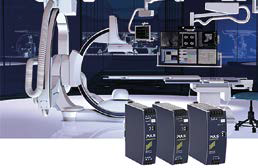
One example of this is XP Power's AQM series, consisting of 200W, 250W and 300W external medical power supplies that take advantage of GaN technology to achieve efficiencies of up to 94%.

Figure 2: XP Power's AQM series is a compact GaN-based power solution for medical applications.
Home healthcare is an important and growing industry, but to achieve its full potential, the power solutions you need must deliver more power in a compact package. Existing technologies like Si are reaching their limits, which is why designers of high-performance solutions are turning to WBG materials like GaN to deliver the compact yet powerful solutions the market needs.
GaN is characterized by lower losses, faster switching, and higher operating temperature than Si, all of which in turn reduce component size and thermal management needs, with a consequent significant increase in power density.


